- 您现在的位置:买卖IC网 > Sheet目录3882 > PIC16F87T-E/ML (Microchip Technology)IC MCU FLASH 4KX14 EEPROM 28QFN
89
8008H–AVR–04/11
ATtiny48/88
12. 16-bit Timer/Counter1 with PWM
12.1
Features
True 16-bit Design (i.e., Allows 16-bit PWM)
Two independent Output Compare Units
Double Buffered Output Compare Registers
One Input Capture Unit
Input Capture Noise Canceler
Clear Timer on Compare Match (Auto Reload)
Glitch-free, Phase Correct Pulse Width Modulator (PWM)
Variable PWM Period
Frequency Generator
External Event Counter
Four independent interrupt Sources (TOV1, OCF1A, OCF1B, and ICF1)
12.2
Overview
Most register and bit references in this section are written in general form, where a lower case
“n” replaces the Timer/Counter number, and a lower case “x” replaces the Output Compare unit
channel. However, when using the register or bit defines in a program, the precise form must be
used, i.e., TCNT1 for accessing Timer/Counter1 counter value and so on.
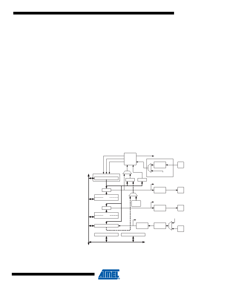
The 16-bit Timer/Counter unit allows accurate program execution timing (event management),
wave generation, and signal timing measurement. A simplified block diagram of the 16-bit
Timer/Counter is shown in Figure 12-1.
Figure 12-1. 16-bit Timer/Counter Block Diagram
Note:
1. Refer to Figure 1-1 on page 2,
Timer/Counter1 pin placement and description.
Clock Select
Timer/Counter
D
ATA
B
U
S
OCRnA
OCRnB
ICRn
=
TCNTn
Waveform
Generation
Waveform
Generation
OCnA
OCnB
Noise
Canceler
ICPn
=
Fixed
TOP
Values
Edge
Detector
Control Logic
= 0
TOP
BOTTOM
Count
Clear
Direction
TOVn
(Int.Req.)
OCnA
(Int.Req.)
OCnB
(Int.Req.)
ICFn (Int.Req.)
TCCRnA
TCCRnB
( From Analog
Comparator Ouput )
Tn
Edge
Detector
( From Prescaler )
clk
Tn
发布紧急采购,3分钟左右您将得到回复。
相关PDF资料
PIC16F87-E/ML
IC MCU FLASH 4KX14 EEPROM 28QFN
PIC18LF4320-I/ML
IC MCU FLASH 4KX16 EEPROM 44QFN
PIC16F77T-I/PTG
IC MCU FLASH 8KX14 W/AD 44TQFP
PIC16LF1933-I/SO
IC PIC MCU FLASH 4K 28-SOIC
PIC16C54C-20I/SO
IC MCU OTP 512X12 18SOIC
PIC16LF726-I/SO
IC PIC MCU FLASH 8K 1.8V 28-SOIC
PIC12CE673-10/P
IC MCU OTP 1KX14 A/D&EE 8DIP
PIC16F726-I/SO
IC PIC MCU FLASH 8KX14 28-SOIC
相关代理商/技术参数
PIC16F87T-E/SO
功能描述:8位微控制器 -MCU 20MHz 4K Flash RoHS:否 制造商:Silicon Labs 核心:8051 处理器系列:C8051F39x 数据总线宽度:8 bit 最大时钟频率:50 MHz 程序存储器大小:16 KB 数据 RAM 大小:1 KB 片上 ADC:Yes 工作电源电压:1.8 V to 3.6 V 工作温度范围:- 40 C to + 105 C 封装 / 箱体:QFN-20 安装风格:SMD/SMT
PIC16F87T-E/SS
功能描述:8位微控制器 -MCU 20MHz 4K Flash RoHS:否 制造商:Silicon Labs 核心:8051 处理器系列:C8051F39x 数据总线宽度:8 bit 最大时钟频率:50 MHz 程序存储器大小:16 KB 数据 RAM 大小:1 KB 片上 ADC:Yes 工作电源电压:1.8 V to 3.6 V 工作温度范围:- 40 C to + 105 C 封装 / 箱体:QFN-20 安装风格:SMD/SMT
PIC16F87T-I/ML
功能描述:8位微控制器 -MCU 7KB 368 RAM 16 I/O RoHS:否 制造商:Silicon Labs 核心:8051 处理器系列:C8051F39x 数据总线宽度:8 bit 最大时钟频率:50 MHz 程序存储器大小:16 KB 数据 RAM 大小:1 KB 片上 ADC:Yes 工作电源电压:1.8 V to 3.6 V 工作温度范围:- 40 C to + 105 C 封装 / 箱体:QFN-20 安装风格:SMD/SMT
PIC16F87T-I/SO
功能描述:8位微控制器 -MCU 7KB 368 RAM 16 I/O RoHS:否 制造商:Silicon Labs 核心:8051 处理器系列:C8051F39x 数据总线宽度:8 bit 最大时钟频率:50 MHz 程序存储器大小:16 KB 数据 RAM 大小:1 KB 片上 ADC:Yes 工作电源电压:1.8 V to 3.6 V 工作温度范围:- 40 C to + 105 C 封装 / 箱体:QFN-20 安装风格:SMD/SMT
PIC16F87T-I/SS
功能描述:8位微控制器 -MCU 7KB 368 RAM 16 I/O RoHS:否 制造商:Silicon Labs 核心:8051 处理器系列:C8051F39x 数据总线宽度:8 bit 最大时钟频率:50 MHz 程序存储器大小:16 KB 数据 RAM 大小:1 KB 片上 ADC:Yes 工作电源电压:1.8 V to 3.6 V 工作温度范围:- 40 C to + 105 C 封装 / 箱体:QFN-20 安装风格:SMD/SMT
PIC16F882-E/ML
功能描述:8位微控制器 -MCU 3.5KB Enh FLSH 128 RAM RoHS:否 制造商:Silicon Labs 核心:8051 处理器系列:C8051F39x 数据总线宽度:8 bit 最大时钟频率:50 MHz 程序存储器大小:16 KB 数据 RAM 大小:1 KB 片上 ADC:Yes 工作电源电压:1.8 V to 3.6 V 工作温度范围:- 40 C to + 105 C 封装 / 箱体:QFN-20 安装风格:SMD/SMT
PIC16F882-E/SO
功能描述:8位微控制器 -MCU 3.5KB Enh FLSH 128 RAM RoHS:否 制造商:Silicon Labs 核心:8051 处理器系列:C8051F39x 数据总线宽度:8 bit 最大时钟频率:50 MHz 程序存储器大小:16 KB 数据 RAM 大小:1 KB 片上 ADC:Yes 工作电源电压:1.8 V to 3.6 V 工作温度范围:- 40 C to + 105 C 封装 / 箱体:QFN-20 安装风格:SMD/SMT
PIC16F882-E/SP
功能描述:8位微控制器 -MCU 3.5KB Enh FLSH 128 RAM RoHS:否 制造商:Silicon Labs 核心:8051 处理器系列:C8051F39x 数据总线宽度:8 bit 最大时钟频率:50 MHz 程序存储器大小:16 KB 数据 RAM 大小:1 KB 片上 ADC:Yes 工作电源电压:1.8 V to 3.6 V 工作温度范围:- 40 C to + 105 C 封装 / 箱体:QFN-20 安装风格:SMD/SMT